Description
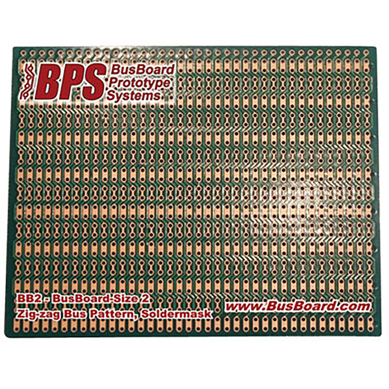
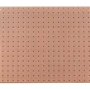
Use the connected pads to lay out a memory bus or connector breakout with fewer point-to-point jumpers.
Specifications
- Single-sided layout
- Solder mask
- 80 × 100 mm
$5.65
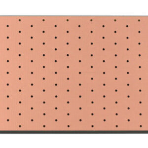
Prototype parallel buses between DIP ICs and dual-row headers. The zigzag copper pattern links corresponding pins while keeping the two rows electrically separate.
Use the connected pads to lay out a memory bus or connector breakout with fewer point-to-point jumpers.
Reviews
There are no reviews yet.